| Difficult | Execution Time | Data Analysis | Radioactive Sources |
|---|---|---|---|
  |
  |
Yes | No |
Purpose of the experiment
This experiment introduces how memory-mapped components can be used inside a sub-design to allow software control and monitoring of FPGA modules.
Fundamentals
In FPGA-based systems, many configuration parameters and measured values are accessed through memory mapped registers. These registers allow software to write configuration values and read measurement results from the firmware. When using sub designs or hierarchical blocks, memory-mapped components can still be accessed from the top-level system. This allows each sub-block to contain its own configuration registers, counters, or memory buffers while remaining accessible to the control software. This approach is commonly used in complex systems where multiple processing blocks must be configured and monitored independently. Students learn how registers and memory blocks inside hierarchical designs can be accessed from software.
Requirements
Python environment.
Carrying out the experiment
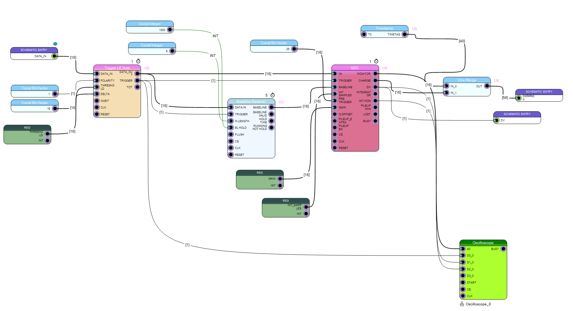
Create a new project for your DT1260 unit by clicking New Project. A firmware design is implemented including a sub-design containing memory-mapped components such as configuration registers, counters, or memory buffers. These components are connected to the main system bus so that they can be accessed from software. Input signals are provided to the board using a pulse generator. The firmware processes the signals, and the values stored in the memory-mapped components can be written or read through the control software.
Results
The system allows software to access and control memory-mapped registers and memory blocks located inside a sub-design. Students can configure parameters and read measurement data from hierarchical blocks within the FPGA design. This experiment demonstrates how memory-mapped components in sub-designs enable flexible configuration and monitoring of complex FPGA-based data acquisition systems.