| Difficult | Execution Time | Data Analysis | Radioactive Sources |
|---|---|---|---|
  |
  |
Yes | No |
Purpose of the experiment
This application demonstrates how to integrate and operate the Oscilloscope block in a Sci-Compiler FPGA design on the DT1260 board, to visualize analog and digital signals in real time.
Fundamentals
An oscilloscope captures and displays signal waveforms, enabling time-domain observation of amplitude versus time. Analog input signals (after ADC conversion) and internal digital signals inside the FPGA can be sampled
and visualized through a memory-mapped interface. Triggering functions (edge detection, thresholds, pre/ post trigger) stabilize the display of periodic or transient signals. A block, called “Oscilloscope”, connects FPGA logic with external visualization tools for debugging and signal validation.
Carrying out the experiment
- Activate your Sci-Compiler license and set up the software installation. Plug the USB Dongle in your PC and launch Sci- Compiler.
- Create a project for your DT1260 unit: press New Project.
- Add the Oscilloscope block to the design and connect analog (A0) and digital (D0–D3) inputs.
- Configure channels, buffer size, and enable capture. Assign memory addresses automatically, build the project, and program the DT1260.
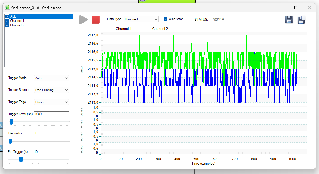
- Feed a test signal (e.g. PWM) to an input, open Oscilloscope_0 from the Resource Explorer, and set trigger source, mode, and level.
- Start acquisition and adjust trigger settings to stabilize the displayed waveform.
Results
The Oscilloscope block provides real-time observation of FPGA-generated signals without external equipment. By adjusting trigger parameters, students can stabilize periodic waveforms or capture transient events, improving signal debugging, timing verification, and system validation.